The most intuitive network for performing spatial smoothing is the one formed using resistive networks. In such networks a resistive grid receives the input current and each node distributes its current among its neighbors. The output can be taken for example by reading the node voltages. We will see that even the most intricate circuits described in this chapter work based on this simple principle.
A simple spatial smoothing circuit, which uses the principle of current distribution into a resistive network is illustrated in Figure 7.27. If all the elements in the network have equivalent impedances, as shown in the figure, one can easily derive the equation relating the output and input currents.

This is a linear recursive transfer function. It can be seen that for
![]()

For ![]() all the output nodes are in fact virtually shorted
and
all the output nodes are in fact virtually shorted
and
![]()
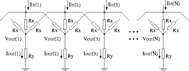
Figure 7.27: Current mode circuit for spatial smoothing.
Implementing such a resistive network would not be economic in standard CMOS processes, because linear passive resistors with large values (to satisfy power consumption constraints) are not readily available. Also, the smoothing constant of the network would be fixed, if all the elements are fixed.
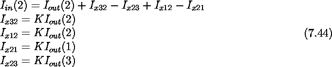
By replacing the resistive elements with translinear elements (e.g. a junction diode or a MOS diode), a more economic circuit can be realized (See figure 7.28). The expressions describing the function of the circuit can be obtained by applying the translinear principle in the loops indicated by dashed lines, and also the KCL at the input and output nodes of the circuit. It is assumed that all the elements are identical. The derivations can be easily extended for a network with different elements values at each branch. Here we only consider this simple case.
A generalized expression can be easily obtained.
Although this is a nonlinear recursive transfer function, the network exhibits a near perfect averaging function similar to a rectangular smoothing window spreading over three neighboring inputs.
A drawback of this circuit is its fixed width of the smoothing operation. The network shown in Figure 7.29 achieves a wider smoothing by using another stage of the current distribution network. Also the middle branch of each stage can be bypassed by a MOS transistor acting as a switch. The smoothing window of this new network can be adjusted to five, three, or zero (no smoothing operation). This circuit has been used for realizing the multiplicative noise cancellation (MNC) operation in the second motion detection chip, which has been described in section 3.11.
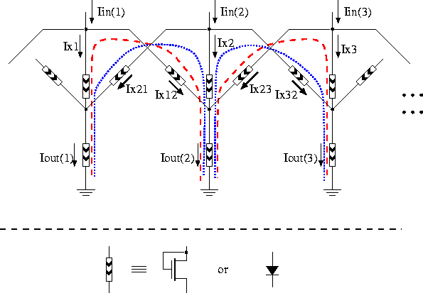
Figure 7.28: A translinear circuit for spatial smoothing.
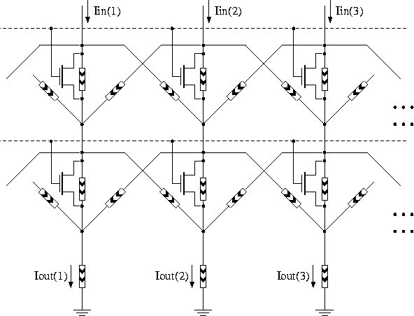
Figure 7.29: Two-stage translinear spatial smoothing circuit.
This circuit can be modified so that the shape of the smoothing window can be adjusted by varying some bias voltages in the circuit. Figure 7.30 illustrates this new idea. Here the transconductance of the transistors is controlled by the gate voltage. The relationship between the output and input currents can be derived as

where  , n is a process dependent
parameter, and
, n is a process dependent
parameter, and ![]() .
.
By using two stages of this circuit (similar to that in Figure 7.29) an adjustable-shape smoothing window covering five neighboring cells can be obtained.
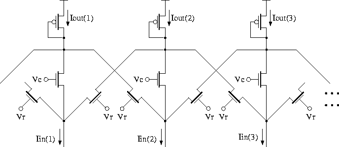
Figure 7.30: Translinear spatial smoothing circuit with adjustable
window shape.
The main drawback of the smoothing circuits described so far is their
fixed window size. A slightly modified version of
Figure 7.30 is shown in
Figure 7.31 (See
[Andreou et al. 91a, Andreou and Boahen 94b, Andreou and Boahen 96]). Note that
the horizontal transistors operate in the ohmic region. This circuit
can be analyzed using the translinear principle by decomposing the
horizontal transistors into two back-to-back transistors operating in
the saturation region (See Figure 7.32).
By writing the translinear equations in the loops marked by dashed
lines (note that the loops end at constant voltages ![]() and
and ![]() )
and the KCL at the circuit nodes we have
)
and the KCL at the circuit nodes we have
where . From these equations we will
have
![]()
![]() is the second spatial-derivative operator. One can easily
work out that the impulse response of this network is an exponentially
decaying function with a decaying rate of
is the second spatial-derivative operator. One can easily
work out that the impulse response of this network is an exponentially
decaying function with a decaying rate of ![]() . One should
notice that this circuit cannot be implemented using bipolar
transistors, as the horizontal MOS transistors operate in the ohmic
region, but all the previous circuits can be implemented using bipolar
transistors without any modification to the structure of the networks.
. One should
notice that this circuit cannot be implemented using bipolar
transistors, as the horizontal MOS transistors operate in the ohmic
region, but all the previous circuits can be implemented using bipolar
transistors without any modification to the structure of the networks.
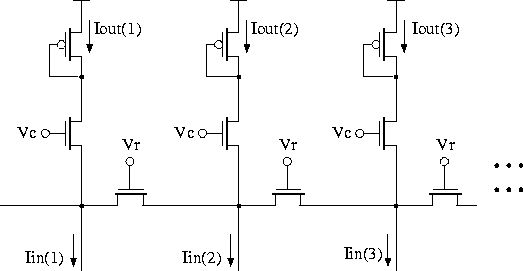
Figure 7.31: Spatial smoothing circuit with adjustable
window width.
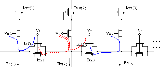
Figure 7.32: Translinear analysis of the smoothing circuit by
decomposing the horizontal transistors into two back-to-back
transistors.
Before ending this section I show another spatial smoothing circuit, again built using the resistive network concept. This circuit was first used for implementing a silicon retina [Mead 89b, Mead and Mahowald 88]. The schematic of the circuit is illustrated in Figure 7.33. The heart of the network is the ``horizontal resistor'' or HRES, which simulates a floating resistor. The OTA-like circuits are used to properly bias the two horizontal transistors. Assuming that some of the circuits are shared between neighboring cells, each cell uses 12 transistors. The circuit designed by Andreou and Boahen [Andreou et al. 91a, Andreou and Boahen 94b] only uses 2 transistors for each cell, a dramatic difference in the number of transistors.
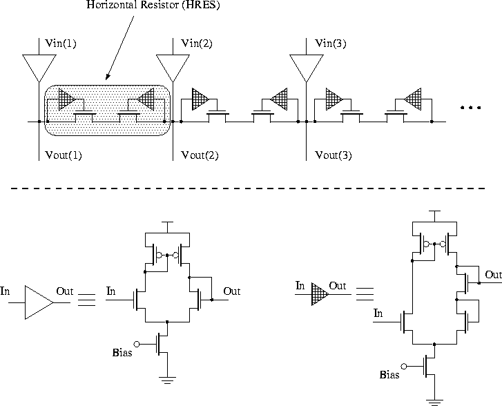
Figure 7.33: Another spatial smoothing circuit, with a large number of
transistors. The OTA at each input converts the input voltage to
a current and injects it into the network. The other OTA-like
circuit (shaded triangle) is used to properly bias the
horizontal transistors.
In this section I presented a series of snapshots of how a very simple and intuitive circuit can be turned into a very useful and powerful one. Of course the evolution of the actual circuits has not followed this straight path, but certainly understanding the principles of the operation of these circuits and the slight variations that has succeeded this evolution can help in building more complex networks. Also, here I have tried to apply the translinear principle as much as possible in analyzing the circuits, and there is virtually no mentioning of the complex transistor equations.