The overall architecture of Near Sensor Image Processing (NSIP) sensor
is very similar to the PASIC (described in section 2.8).
However, it embeds an interesting function for each pixel, which
perform both an A-to-D conversion, and a 1/x
compression [Forchheimer and Åström 94, Forchheimer and Åström 92, Åström et al. 96, Åström 93].
The schematic diagram of a pixel is shown in
Figure 2.13. The photodetector works in integration
mode. By applying the Reset signal the voltage at the input node
![]() is precharged to
is precharged to ![]() . By turning off the resetting
transistor,
. By turning off the resetting
transistor, ![]() charges up and when it reaches the reference
voltage
charges up and when it reaches the reference
voltage ![]() the output voltage becomes high. The time that it
takes from the onset of the charging until the output voltage becomes
high is related to the input light intensity (input photocurrent) by:
the output voltage becomes high. The time that it
takes from the onset of the charging until the output voltage becomes
high is related to the input light intensity (input photocurrent) by:
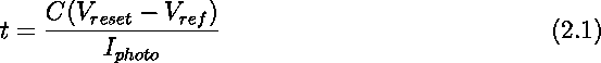
Therefore, if the output of the detectors are sampled at some intervals, after resetting the sensor array, the intensity at each detector can be derived from the sample number at which the output of the detector has become high.
For imaging applications the readout mechanism would be complicated, as all the detectors should be read at small sampling periods and their status should be registered in a memory. However, for some image processing tasks, for example finding the position of the maximum intensity, or detecting positive or negative gradients, this method of reading the output at samll periods and performing micro-instructions on the outputs, proves more economic than the traditional methods.
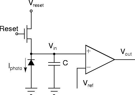
Figure 2.13: The photocircuit of the NSIP sensor.