This foveated sensor has been designed by several groups from the University of Genoa, Italy, University of Pennsylvania-USA, Scoula Superiore S Anna of Pisa, and has been fabricated by IMEC in Leuven, Belgium [van der Spiegel et al. 89, Pardo and Martinuzzi 94]. It features a unique concept in the VLSI implementation of a vision chip. The foveated chip, which uses a CCD process, mimics the physically foveated (versus optically foveated, as in some birds) retina of human. Foveated vision is known to reduce the amount of information passed to subsequent processing layers significantly and therefore lends itself to image processing and pattern recognition tasks which are currently performed using uniformly spaced imagers. The foveated vision, however, has evolved concurrently with the eye motor system, where fovea focuses on areas of interest. This can be best utilized for robotic applications in which the low resolution periphery of the fovea finds areas of interest, and then directs the foveated part to get the details of those areas.
The chip has a foveated rectangular region in the middle with high resolution and a circular outer layer with decreasing resolution. The chip floor plan in Figure 2.14 shows different regions of the chip. In the circular region the chip implements a log-polar mapping of the Cartesian coordinates. This mapping provides a scale and rotation invariant transformation.
The chip has been fabricated using a triple-poly buried channel CCD
process provided by IMEC. The rectangular inner region has 102
photodetectors. There are 30 eccentric circular layers in the
peripheral part, each having 64 photodetectors. A part of the circles
has been sliced to allow the interconnection of clock and control
signals. The chip area is 11mm ![]() 11mm. In
references [van der Spiegel et al. 89, Pardo and Martinuzzi 94] other aspects of the design,
such as read-out structures, clock generation, simple theories about
the fovea, and hardware interface to the chip are described.
11mm. In
references [van der Spiegel et al. 89, Pardo and Martinuzzi 94] other aspects of the design,
such as read-out structures, clock generation, simple theories about
the fovea, and hardware interface to the chip are described.
Other features of this chip are:
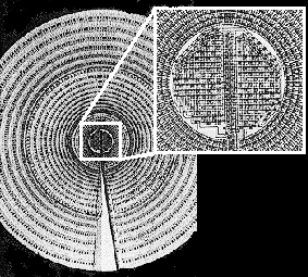
Figure 2.14: Photograph of the foveated CCD retina.
To obtain a relevant PS document provided by Fernando Pardo (ftp from Adelaide 160K)