The pixel circuit (photocircuit) in active pixel sensors are often based on the charge integration method (See section 7.3.8). The photodetector structure used for APS can also be based on any of the photodetector structures described in section 7.2. The read-out circuit used in APS is often a source follower based circuit described in section 7.9.1. In fact there is very little amount of new concepts in APS.
Figure 7.24 illustrates two of the common photocircuits used in APS. In the photogate-based circuit initially the node X is reset and charge starts integrating in the the potential well under the photogate created by applying a large voltage to the gate of the photogate device. After the integration cycle the charge is transferred to node X and read out. In the photodiode-based circuit after the reset operation charge is continuously integrated on the node X until the next reset. Notice that there is no Sample&Hold stage in either of these photocircuits, and in reality while the output of some of the photocircuits are being read out other photocircuits are still integrating charge. In simple imagers this does not impose any problems, as the read-out time is much shorter than the integration time.
The advantages and disadvantages of both structures are as follows.
In the illustrated photodiode-based circuit the integration and reset nodes are the same. Therefore, it is not possible to perform the correlated double sampling operation in the same frame period. In order to add this facility to the photodiode-based circuit, a transfer gate similar to the photogate-based circuit, can be added to this circuit.
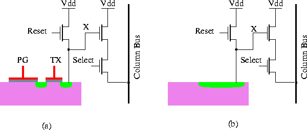
Figure 7.24: a) APS photocircuit using a photogate. b) Using a photodiode.