Almost all commercially available imagers and some of the vision chips
described in this report use charge integration and sample-&-hold for
transducing the photocurrent into a voltage. The basic diagram for
this photocircuit is shown in Figure 7.23. Initially
the reset transistor is on and the voltage at the input node In is
set to the reset value. Then this transistor is turned off and the
photocurrent charges up the input capacitance at the input node. The
input capacitance is usually comprised of the parasitic capacitances
of the devices connected to this node. In some processes, e.g. GaAs,
which have a large gate leakage current, an additional capacitor,
![]() may be needed to ensure enough charge storage time.
may be needed to ensure enough charge storage time.
The sample and hold stage can often be removed. However, in this case after resetting the detector array and during the read-out process, some of the detectors still integrate charge while others are being read out. For simple imaging applications this does not impose serious problems, as the read out time is usually very short.
Charge integration method has several advantages and disadvantages. The advantages are its linear transfer characteristics, controllable dynamic range by changing the integration time, and low sensitivity to device mismatch at least up to the S&H stage because the integration time depends on the input capacitance which has less mismatch than other parameters of the circuit. Also the integration principally acts as a low-pass filter which removes the high frequency components of the noise (both the device noise and the digital noise).
The main disadvantages of this method are its inability to locally change the integration time, which means that the dynamic range for a specific integration time is always limited to a certain global value. However, recent progress in the design of smart sensors have made it possible to control the integration time of individual pixels at the expense of some area [Chen and Ginosar 95, Chen and Ginosar 96].
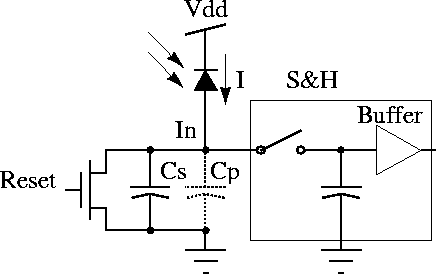
Figure 7.23: Integration based photocircuit.