Adopting a certain test strategy is important for a vision chip, although it is often neglected as a side-issue. This could be because of the nature of the vision chips being designed so far, as the majority have been research prototypes with emphasis on the algorithm implementation or circuit design techniques, rather than system integration and interfacing.
Some of the important issues that may be considered in relation to testing are listed below.
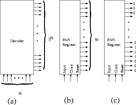
Figure 7.43: a) Decoder based random access scanning. b) shift register-based
serial scanning. c) Using shift register scanning to select
several cells at a time.
For current and voltage read-out there are many circuits available. One should make sure that the operating range of these circuits matches to the range of the output signals of the vision chip array. Specially for current read-out circuits the range may be several decades. If the current levels are very low, in the order of pico and nano amperes, the read-out circuits should be very sensitive and special read-out schemes should be used.
A voltage read-out circuit that is widely used in active pixel sensors consists of the input transistor of a source follower included in the photocircuit and the biasing transistor common for all the pixels. The circuit schematic is shown in Figure 7.44.
Current read-out in the simplest form can be performed using a resistive element, either passive or active. In either case as the voltage at the read-out node will depend on the current level, and the charge and discharge time also depends on the current, very slow responses would be expected for small currents, which are very common in many vision chips. A better circuit for reading current is shown in Figure 7.45-b. In this circuit the voltage at the read-out node is fixed using the Op-Amp. Hence the current does not need to charge or discharge this node. Instead of a linear resistor in the feedback loop, an element with a logarithmic characteristics (a MOS or junction diode) can be used. This is specially useful for reading currents which vary over several decades. If a capacitor is used instead of the resistor, as shown in Figure 7.45-c, a charge integration read-put is obtained. This circuit is very widely used in current read-out circuits, due to its linearity.
If the algorithm and architecture allows it is often easier to use the charge integration technique (the same as in integration-based photocircuits) to perform a linear current-to-voltage transformation at the pixel level(See Figure 7.45-d). This will alleviate many of the requirements for current read-out circuits.
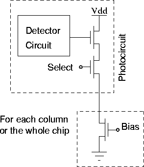
Figure 7.44: A voltage read-out circuit using a source follower.
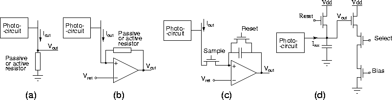
Figure 7.45: Current read-out circuits. a) Using a simple resistive load.
b) Using active current read-out. The voltage at the read-out node
is fixed at ![]() . c) Using charge integration at each column
or for whole chip. d) Using pixel level charge integration.
. c) Using charge integration at each column
or for whole chip. d) Using pixel level charge integration.
In addition to the type of ADC the number of ADC circuits that can be implemented on the chip can also be selected based on demand. If a parallel ADC method is used, as described in section 2.8, the speed requirement of the ADC components will be reduced by the number of columns in the array. Other alternatives in choosing the number of ADC circuits are to use only one ADC for the whole chip, or use multiple ADCs (but less than the number of columns). Torelli shows that in many respects (power, area, and resolution) there is not much gain from using any of these architectures. However, a single ADC will avoid the addition of fixed pattern noise, which can be introduced by multiple ADCs. On the other hand, the less speed demanding feature of multiple ADCs may be considered as an advantage.