Shunting inhibition (SI), or multiplicative lateral inhibition, is known to be one of the models of the retina which demonstrates many its functional behaviors. In order to investigate the properties of a silicon implementation for shunting inhibition, a chip containing feedback and feedforward shunting inhibition models have been implemented [Moini et al. 97a]. This design uses current mode techniques and subthreshold circuits to implement the complete SI equation including the temporal component.

where ![]() is the output of cell i,
is the output of cell i, ![]() is the input, b is a
decay factor, and k is the inhibition factor. The building block of
a cell in the feedback SI is shown in Figure 3.36. In
the feedforward circuit copies of the input current of the neighboring
cells are involved in the inhibition, instead of copies of the output
currents. The current mode temporal differentiator circuit is shown in
Figure 3.37. The circuit is based on the current
delay using an OTA-C element. The multiplier/divider circuit is the
same as that shown in Figure 3.15 in
section 3.11.
is the input, b is a
decay factor, and k is the inhibition factor. The building block of
a cell in the feedback SI is shown in Figure 3.36. In
the feedforward circuit copies of the input current of the neighboring
cells are involved in the inhibition, instead of copies of the output
currents. The current mode temporal differentiator circuit is shown in
Figure 3.37. The circuit is based on the current
delay using an OTA-C element. The multiplier/divider circuit is the
same as that shown in Figure 3.15 in
section 3.11.
The chip contains several 64 ![]() 1 arrays of different
implementations of the SI circuits. It has been fabricated in a 2P-2M
2
1 arrays of different
implementations of the SI circuits. It has been fabricated in a 2P-2M
2 ![]() m CMOS process, in an area of 4.6mm
m CMOS process, in an area of 4.6mm ![]() 6.8mm. The height of
each cell is 57mum.
6.8mm. The height of
each cell is 57mum.
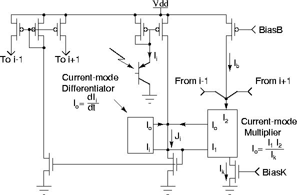
Figure 3.36: Moini et al.'s feedback shunting inhibition circuit.
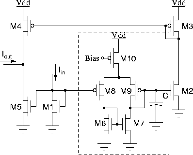
Figure 3.37: a) Current mode differentiator. b) Current mode
divider/multiplier.