The 2D CCD/CMOS imager and processor designed by Keast and Sodini [Keast and Sodini 92, Keast and Sodini 93, Keast and Sodini 90] combines the CCD imager and CMOS processing blocks to perform smoothing and segmentation on the input image. A simplified schematic of several cells of the chip are shown in Figure 2.26. Each cell comprises a CCD photodetector, and several other CCD elements. A CCD/CMOS circuit also computes the difference between two neighbors. If the difference does not exceeds a predefined threshold, the gate of a mixing CCD device (shown in green color) is connected to a proper clock to perform a smoothing operation. Otherwise, the gate of the mixing CCD device is connected to another clock, as a result of which no smoothing is performed. Calculating the difference and comparing it with a threshold is done using the absolute value of difference circuit (AVD) described in section 4.2. The smoothing operation is performed by a fill-and-spill CCD circuit described in section 3.12.
The fabricated chip comprises a 4 ![]() 4 array on cells. It is
designed in a 2
4 array on cells. It is
designed in a 2 ![]() m buried channel CCD/CMOS process.
m buried channel CCD/CMOS process.
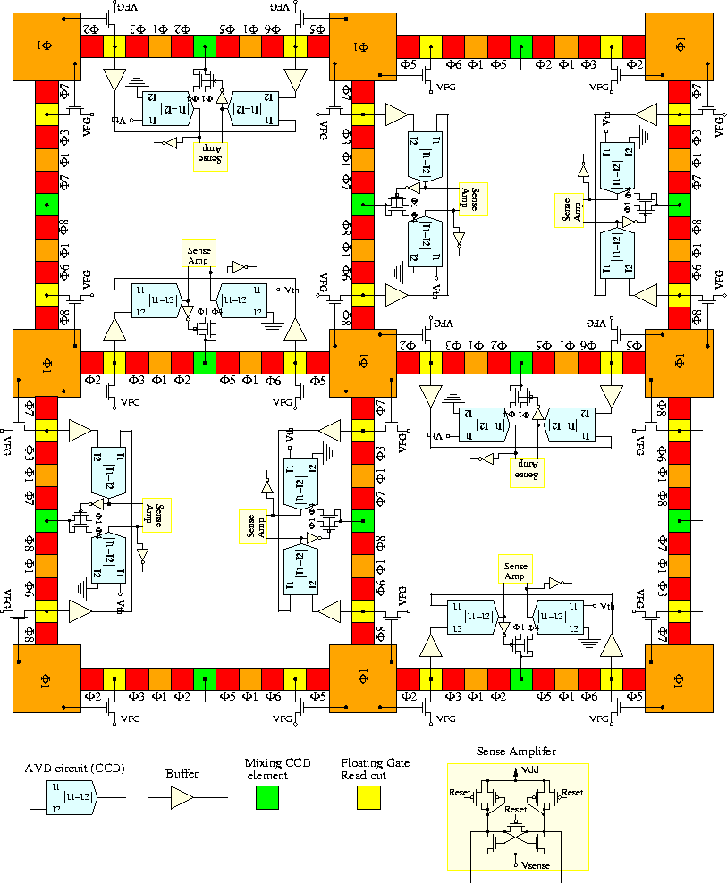
Figure 2.26: The architecture of Keast-Sodini's CCD/CMOS segmentation chip.