In [Hakkaranien and Lee 93, Hakkaranien et al. 91] Hakkaranien and Lee describe a CCD/CMOS chip for computing one of the stages in processing stereo vision. In implementing the Marr-Poggio-Drumheller algorithm for stereo vision, four processing steps are required.
The chip only implements the second step. It comprises a CCD input stage, CCD shift registers, floating-gate output stage for non-destructive read out, absolute value of difference (AVD) circuit, CCD memory for storing the output of AVD stage, and a floating-diffusion output stage. The architecture is shown in Figure 4.1. The main part, i.e. the AVD cells generate an absolute value of difference of two pixels from the left and right images. It is composed of two cross coupled fill-and-spill CCD circuits, shown in Figure 4.2. Considering only the CCD elements connected to VL and VR it can easily be seen that when VR > VL the potential well of the left fill-and-spill circuit retains a charge proportional to the difference of VL and VR, while the right fill-and-spill circuit becomes empty.
The chip has a 40 ![]() 40 array of match generators. It has been
designed using a 2
40 array of match generators. It has been
designed using a 2 ![]() CCD/CMOS process in an area of
7.4mm
CCD/CMOS process in an area of
7.4mm ![]() 8.7mm, and dissipates 450mW.
8.7mm, and dissipates 450mW.
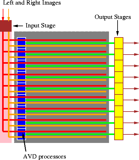
Figure 4.1: Architecture of Hakkaranien-Lee's vision chip.
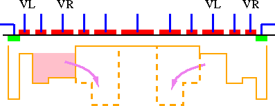
Figure 4.2: The AVD cross section showing potential wells when VR >
VL.