In conventional methods modulating an image with a desired kernel is performed after the photodetection stage. In Mitsubishi's CMOS retina chips, the photocurrent output from photodetectors is directly modulated, therefore obviating post-detector processing [Funatsu et al. 94, Funatsu et al. 95a, Funatsu et al. 95b, Funatsu et al. 96]. GaAs based variable sensitivity photodetectors (VSP) have also been used in retina chips based on this concept [Nitta et al. 95, Lange et al. 93](See section 5.1).
The circuit of a pixel is shown in Figure 2.27. The output of the photodetector determines the bias current of the OTA. The output current of the OTA depends on the input differential voltage and the bias current.

Therefore a simple and effective modulation of the input image can be obtained. The read-out mechanism selects several pixels in a column at the same time and applies proper voltages to the input of the corresponding OTAs, thereby convolving the image with a kernel. As the applied voltages can be selected arbitrarily, a vast number of image processing tasks, such as edge detection and smoothing, can be performed using this retina.
The fabricated chip has 256 ![]() 256 pixels of VSP detectors with
dimension of
256 pixels of VSP detectors with
dimension of ![]() , in a 2
, in a 2 ![]() m 1P-2M NMOS process.
m 1P-2M NMOS process.
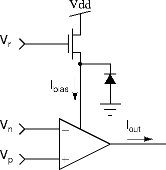
Figure 2.27: Pixel circuit of a MOS VSP detector.