One of the best photocircuits which satisfies many desired static and dynamic characteristics is the Delbrück's adaptive photocircuit. This photocircuit which is described in great detail in [Mead 94] can adapt to steady state (or long term) light intensity variations through a logarithmic transfer function, while having a large gain for short term variations.
The circuit is principally based on the photocircuit using buffering pull-up, described in section 7.3.2. However, in the feedback loop from the output of the amplifier an adaptive element and a capacitive voltage divider has been used. The adaptation function of this photocircuit depends on the characteristics of the adaptive element shown as a shaded box in Figure 7.19. If we assume that it is just an extremely large resistor, one can easily see that at low frequencies the circuit operates similar to the buffering pull-up photocircuit. At higher frequencies the gain of the circuit is boosted by the capacitive division of C1 and C2. The circuit is therefore capable of providing high gain for short term signals which are usually of more importance than long term signals. Long term signals are logarithmically compressed.
An important component of this photocircuit is the adaptive element. Delbrück presents several structures for this element (shown in Figure 7.20) and argues, through experimental and analytical data, that the best choice is the structure in Figure 7.20-f. The choice has been made based on the leakage and offset current of these elements.
These adaptive elements, in addition to demonstrating a very large impedance at small voltages, allow a large current to pass at large voltages ( > 0.5 volt). This is useful for damping transients resulting from large input variations.
It should be noticed, however, that this circuit is useful for vision chips which require an amplified input for temporal processing. In other words, the higher gain for higher temporal frequencies will distort the original image, and therefore if such a photocircuit is used in imagers, this distortion should be taken into account. The best position for this photocircuit is in motion detection vision chips, as often in these chips there is a pressing requirement for high gain and high temporal contrast.
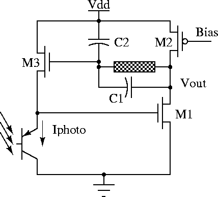
Figure 7.19: The circuit diagram of the adaptive photodetector.
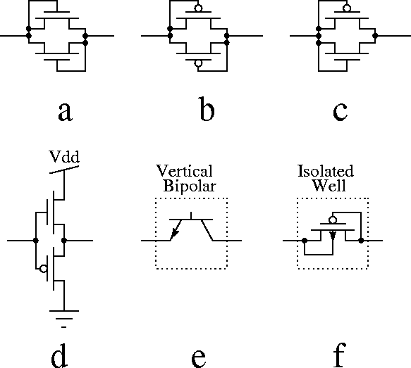
Figure 7.20: The circuit diagram of the adaptive photodetector.