Compensating the capacitive load present at the input node of the photodetector is essential for enhancing the dynamic response of the photocircuit, specially when either the input current in very low or the capacitive load is large. A method that has been used in several vision chips but with different topologies is shown in Figure 7.16.
The small signal operation of the circuit can be easily understood by deriving its transfer characteristics.
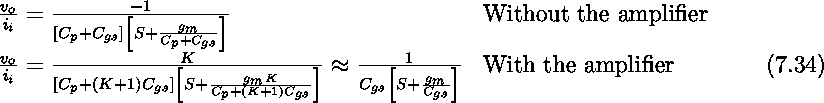
As is seen, the pole of the photocircuit with the amplifier in the
feedback loop is transferred to a new location instead of gm/Cp.
The gain is also enhanced. It should be mentioned that the pole
location still depends on the input current level as we have ![]() in subthreshold.
in subthreshold.
The DC operating point of this photocircuit is mainly determined by the amplifier. For example, if a symmetric inverter (a CMOS inverter with the transition region at Vdd/2) is used, the voltage at Vi will settle at Vdd/2. If a high gain differential amplifier is used with its positive input connected to a reference voltage, Vi will be set at that reference voltage. However, notice that the DC value of the output voltage Vo always depends on the input photocurrent, and if the reference voltage mentioned above is constant the, output voltage will have a logarithmic function versus the input photocurrent. This means that the circuit still performs as a logarithmic compressor.
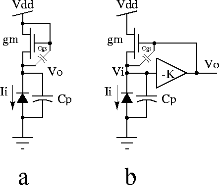
Figure 7.16: a) Without an amplifier in the feedback loop. b) Buffering
photocircuit with an amplifier in the feedback loop.