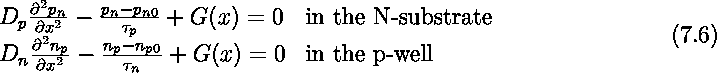
For the structure shown in Figure 7.2, the photocurrent is composed of two components: the drift current due to the drift of holes and electrons in the depletion region, and the diffusion current due to the diffusion of carriers outside the depletion region ([Moini 94]).
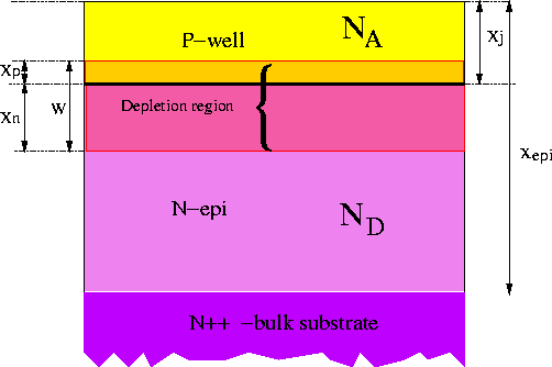
Figure 7.2: The structure of a junction photodetector. ![]() is the
metallurgical junction depth, W is the width of the depletion
region, and
is the
metallurgical junction depth, W is the width of the depletion
region, and ![]() is the thickness of the epitaxial layer.
is the thickness of the epitaxial layer.
The drift current in the depletion region is:

where G(x) is the carrier generation rate for an incident photon
flux, ![]() , in a semiconductor with an absorption coefficient of
, in a semiconductor with an absorption coefficient of
![]() , and is given by
, and is given by
![]()
Hence
![]()
![]() and
and ![]() are the depletion region extents in the n and p sides
of the junction and are given by
are the depletion region extents in the n and p sides
of the junction and are given by
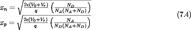
where ![]() is the reverse bias voltage applied to the junction, and
is the reverse bias voltage applied to the junction, and
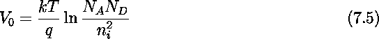
![]() is the built-in potential of the junction and is equal to
is the built-in potential of the junction and is equal to
The diffusion component of the current can be found from the diffusion equation:
where ![]() and
and ![]() are the diffusion coefficients of the minority
carriers,
are the diffusion coefficients of the minority
carriers, ![]() and
and ![]() are the lifetime of excess carriers,
and
are the lifetime of excess carriers,
and ![]()
![]() are the equilibrium minority carrier densities.
The above equation can be solved under the boundary conditions
are the equilibrium minority carrier densities.
The above equation can be solved under the boundary conditions
![]() ,
, ![]() ,
, ![]() , and
, and
![]() to obtain
to obtain

where ![]() and
and ![]() are the diffusion lengths of excess carriers,
and
are the diffusion lengths of excess carriers,
and
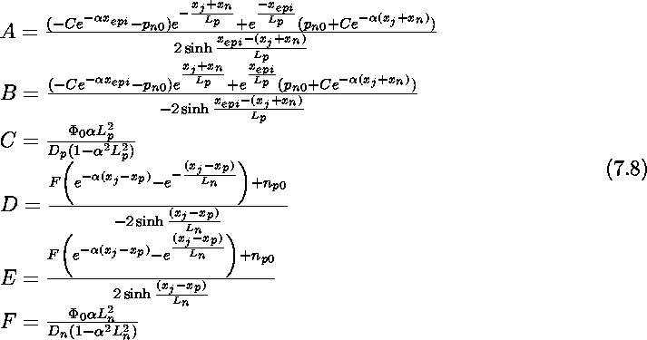
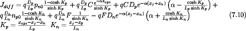
The diffusion current can be found as
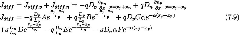
which can be simplified as
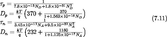
The parameters ![]() ,
, ![]() ,
, ![]() , and
, and ![]() can be derived
from the following empirical formulas for silicon, as a function of
impurity densities
can be derived
from the following empirical formulas for silicon, as a function of
impurity densities
The total current is the summation of the drift and diffusion currents.
![]()
The above equations can be simplified for single-sided and shallow
junctions for a better understanding of the effect of different
parameters on the photoresponse of the device, but we keep them in
their general form. The measured absorption coefficients for silicon
is shown in Figure 7.3. Typical parameters of
a p-well-substrate and a diffusion-well silicon junctions are shown
in Table 7.1. The simulated quantum efficiency,
![]() , for these devices is plotted in
Figure 7.4. As is seen the quantum efficiency of the
diffusion-substrate junction is more than the other two structures and
it also spans over a wider spectrum.
, for these devices is plotted in
Figure 7.4. As is seen the quantum efficiency of the
diffusion-substrate junction is more than the other two structures and
it also spans over a wider spectrum.
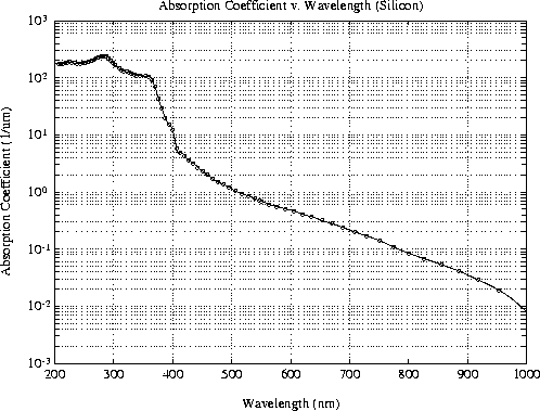
Figure 7.3: Measured absorption coefficient of silicon.
Diode structure ![]()
![]()
![]()
![]()
![]()
![]()
![]()
![]()
![]()
![]()
![]()
![]()
volts ![]()
![]()
![]()
p-well-substrate 2.25 10-15 ![]()
![]()
0 ![]()
199.6 694 n-diff-p-well 0.47 2.25 ![]()
![]()
0 ![]()
199.6 0.71 p-diff-substrate 0.47 10-15 ![]()
![]()
0 ![]()
446.8 0.289 ![]() m p-well standard
process provided by Orbit Semiconductor Inc.
m p-well standard
process provided by Orbit Semiconductor Inc.
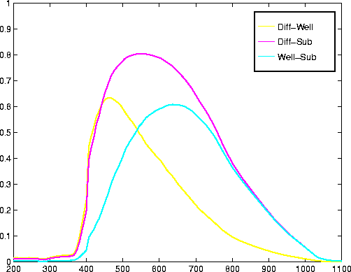
Figure 7.4: Simulated quantum efficiency versus wavelength for three
different junction diodes in a 2 ![]() m process.
m process.