The structure of a lateral photodiode is shown in
Figure 7.5. Before analyzing the devices
photoresponse we make a few simplifying assumptions. We assume that
only the area between the two diffusions is exposed to the light.
Because otherwise, there will be a large contribution from the
vertical bipolar component formed by p-diffusion/n-well/p-substrate.
In reality the photogenerated electron-hole pairs will diffuse to
other areas. We also assume that the effective depth of the device is
only ![]() . Again there will be some currents diffusing through other
areas.
. Again there will be some currents diffusing through other
areas.
The diffusion equations in the p+ and n-well are
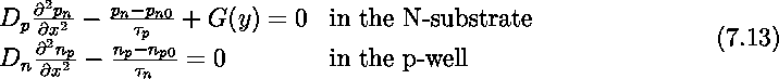
By solving these equations and the boundary conditions ![]() and
and ![]() , we will have
, we will have
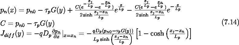
The drift current is simply
![]()
The total current can be obtained by integrating the addition of the drift and diffusion components across the depth and width of the device.
![]()
where
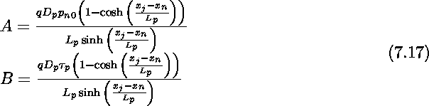
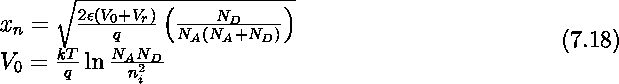
Figure 7.6 shows the simulation result of
this structure for a typical 2 ![]() m process. As one may expect there
is a large blue response, as all the carriers generated close to the
surface are absorbed by the device. The poor response as larger
wavelengths is due to the fact the we have considered the contribution
of those carriers only y-j deep into the device, which is very
shallow. One can combine this structure with the vertical photodiode,
by exposing all sides of the diode to the light.
m process. As one may expect there
is a large blue response, as all the carriers generated close to the
surface are absorbed by the device. The poor response as larger
wavelengths is due to the fact the we have considered the contribution
of those carriers only y-j deep into the device, which is very
shallow. One can combine this structure with the vertical photodiode,
by exposing all sides of the diode to the light.
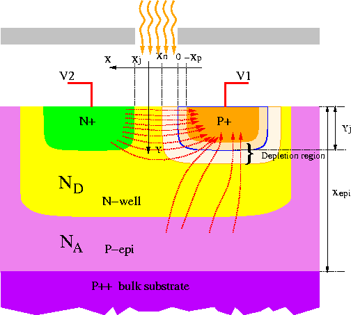
Figure 7.5: The structure of a lateral junction diode in an N-Well CMOS
process.
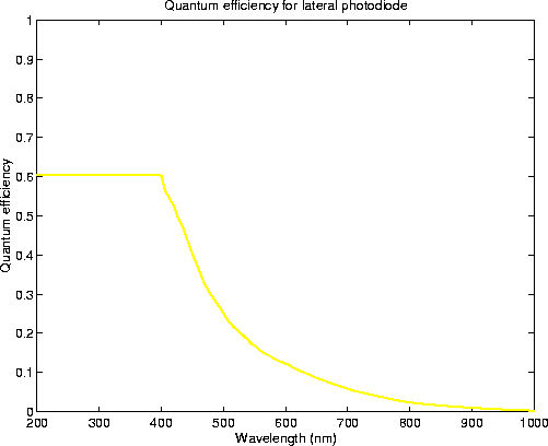
Figure 7.6: Simulation result of the lateral photodiode in a 2 ![]() m CMOS
process.
m CMOS
process.