The structure of a vertical bipolar transistor is shown in Figure 7.7. We assume that only the flat area is exposed to the light. Because otherwise, there will be some contribution from the vertical walls of the emitter-base and base-collector junctions.
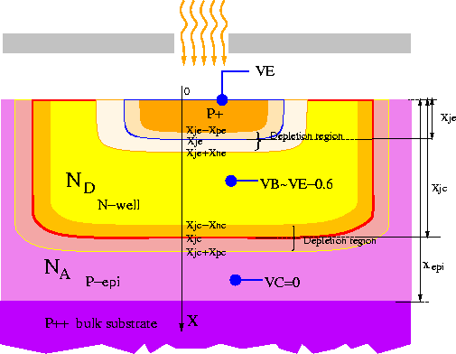
Figure 7.7: The structure of a vertical bipolar detector in an N-Well CMOS
process.
We can write the diffusion equation in the three regions as:
The boundary conditions are:
The diffusion equations can easily be solved.
The diffusion component of the emitter and collector currents can be found by

The drift components can simply be obtained by integrating the amount of generated electron-hole pairs in the depletion regions.
As the base of this device is floating the collector and emitter
currents should be equal. The only variable parameter, which is
unknown is ![]() . The value of
. The value of ![]() for which
for which ![]() can be
found using numerical methods. Figure 7.8
shows the quantum efficiency of a typical parasitic PNP transistor in
a 2
can be
found using numerical methods. Figure 7.8
shows the quantum efficiency of a typical parasitic PNP transistor in
a 2 ![]() m process. The large gain is simply due to the current gain of
the bipolar transistor, which is larger than one. Simulation reveal
that the current gain is highly dependent on the base and emitter
doping densities. As one could expect the response is relatively flat
over the visible spectrum. This is a result of having two junctions at
two different depths in the device.
m process. The large gain is simply due to the current gain of
the bipolar transistor, which is larger than one. Simulation reveal
that the current gain is highly dependent on the base and emitter
doping densities. As one could expect the response is relatively flat
over the visible spectrum. This is a result of having two junctions at
two different depths in the device.
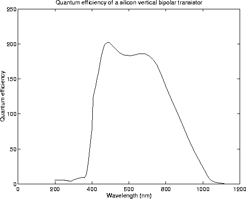
Figure 7.8: Simulated quantum efficiency of a vertical bipolar transistor
in a 2 ![]() m CMOS process. Note that the quantum efficiency is
greater than ``1'', due to the current gain of the transistor.
m CMOS process. Note that the quantum efficiency is
greater than ``1'', due to the current gain of the transistor.