The structure of a lateral bipolar device is shown in
Figure 7.9. Before analyzing the devices
photoresponse we make a few simplifying assumptions. We assume that
only the area between the emitter and collector diffusions, and the
depletion regions are exposed to the light. Because otherwise, there
will be a large contribution from the vertical bipolar components
formed by p-diffusion/n-well/p-substrate. In reality the
photogenerated electron-hole pairs will diffuse to other areas. We
also assume that the effective depth of the device is only ![]() .
Again there will be some currents diffusing through other areas.
.
Again there will be some currents diffusing through other areas.
Note that in the equations x denotes the horizontal axis and y the
vertical axis. Also ![]() is the depth of the collector/emitter
junctions.
is the depth of the collector/emitter
junctions.
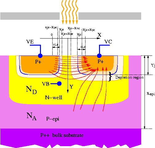
Figure 7.9: The structure of a lateral bipolar detector in an N-Well CMOS
process.
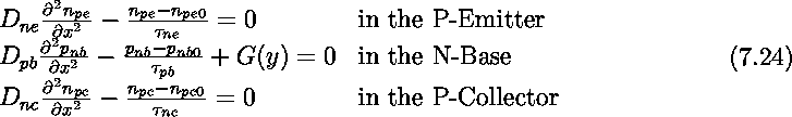
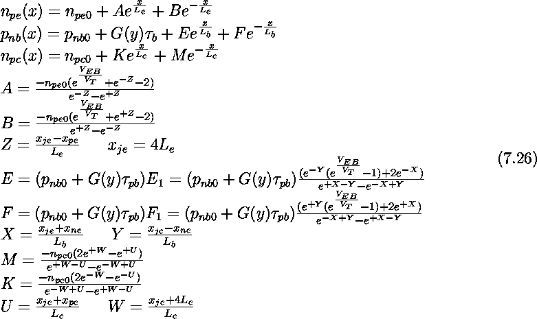
The diffusion equations in three regions can be written as:
The diffusion length in the collector and emitter regions is very
short. Therefore, we make another simplifying assumption that these
junctions extend four times the diffusion length in these regions. We
set the origin at ![]() before the start of the emitter junction, to
be able to reuse the derivations for the vertical bipolar transistor.
before the start of the emitter junction, to
be able to reuse the derivations for the vertical bipolar transistor.
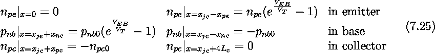
The boundary conditions for the three regions are:
The diffusion currents at collector and emitter are:

The drift currents in depletion regions of the collector and emitter junctions are:

The emitter and collector currents can be obtained by integrating the
corresponding drift and diffusion components of each current over the
range ![]() . Notice that the current density is
per unit width of the device. These should be divided by the junction
depth
. Notice that the current density is
per unit width of the device. These should be divided by the junction
depth ![]() to yield a current density per unit area. The simulation
result for a PNP device with minimum diffusion spacing (
to yield a current density per unit area. The simulation
result for a PNP device with minimum diffusion spacing ( ![]() ) in
a 2
) in
a 2 ![]() m CMOS process is shown in
Figure 7.10. The general shape of the quantum
efficiency is very similar to that of a lateral photodiode
(Figure 7.6).
m CMOS process is shown in
Figure 7.10. The general shape of the quantum
efficiency is very similar to that of a lateral photodiode
(Figure 7.6).
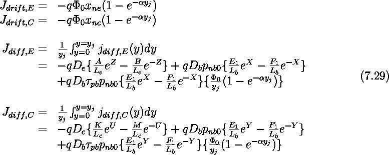
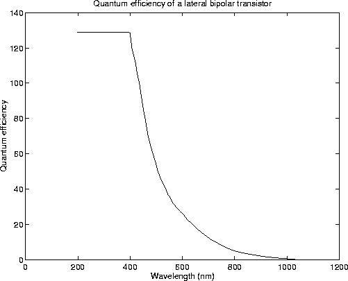
Figure 7.10: Simulated quantum efficiency of a vertical bipolar transistor
in a 2 ![]() m CMOS process.
m CMOS process.