In this section a general view of various photodetector elements(PD), which have been used for vision chips is provided. This view will be limited only to those photodetectors available in standard processes; in other words, only parasitic elements which can be utilized as photodetector. In CCD, CMOS, and GaAs processes there can be found at least one form of junction diode that can serve as a photodetector. CCD processes have more mature forms of photodetectors simply because of the large demand on CCD cameras. CMOS and GaAs, on the other hand, have been paid less attention in the profitable world of imaging. However, the advancement of vision chips in industrial applications, and the very resourceful circuit and device libraries of CMOS processes is going to change this and attract more attention.
In a standard CMOS process, either p-well or n-well, several parasitic junction devices can be used as photodetecting elements, depicted in Figure 7.1. The first three structures are junction diodes, the fourth one is a parasitic vertical bipolar transistor, and the fifth structure is capable of bidirectional photocurrent generation depending on the voltage across the device. The fifth structure can also be considered as a lateral bipolar transistor with symmetric emitter and collector. The last structure is a photogate which in fact has been borrowed from CCD processes. The photogenerated charges are stored in a potential well, produced by applying a large voltage to the gate of the device.
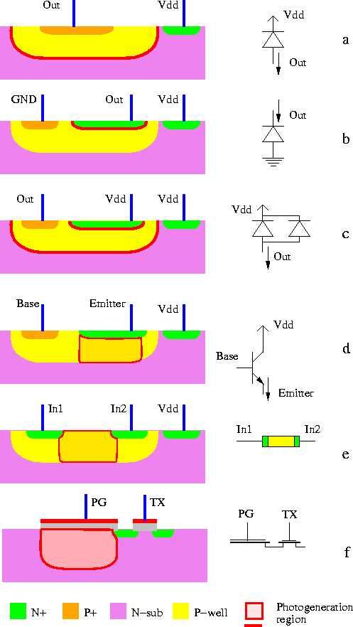
Figure 7.1: a) well-substrate junction diode, b) diffusion-well diode, c)
well-substrate and diffusion-well diodes in parallel, d) vertical
bipolar transistor, e) bidirectional photodetector, and f)
photogate.
Each of these structures can be analyzed in detail relatively easily. Here we provide analysis for each device, and derive equations for the quantum efficiency as a function of geometrical and metallurgical parameters of them. Note that there are several simplifying assumptions made for each structure. The general assumptions made in all the derivation in the following sections are:
In order to improve the consistency between the simulation results from the derived equations and the real measured data one can take the above parameters into account. However, the derived equations can still provide a good insight into the operation of these devices, and illustrate the effect of different parameters on the quantum efficiency. Also for almost all processes, there are no accurate data available for the physical and metallurgical parameters of the process. Therefore, it is rather unnecessary to be concerned about some of these effects. In the extreme case one can use device simulation softwares to numerically derive the device characteristics.