The function of many vision chips may be viewed as modulating the input light intensity using some circuits. By utilizing spatial light modulators (SLM) part of this modulation can be performed by these devices. The general idea is in fact the same as the variable sensitivity detectors(VSD) described in section 5.1. The two concepts are illustrated in Figure 5.2. In SLMs a layer of ferroelectric liquid crystal (FLC) material is encapsulated between the chip and glass cover. The main advantage of ``FLC on silicon'' over GaAs optical neuro-chips, is its higher contrast and lower cost [Yu et al. 95a, Yu et al. 96a, Yu et al. 96b, Yu et al. 95b].
Schematic diagram of a pixel of the chip designed by Yu et al. is
shown in Figure 5.3. X, T, Y, and W are the
input, target output, actual output, and weight of the pixel. Using
this circuit an iterative delta learning is implemented. The
five-transistor OTA computes the required ![]() from the target
and actual outputs, and changes the voltage at the LC pad. The LC pad
is a square metal from which the input light, X, is reflected and at
the same time modulated by the orientation of the FLC crystals, which
depends on the voltage applied to the pad.
from the target
and actual outputs, and changes the voltage at the LC pad. The LC pad
is a square metal from which the input light, X, is reflected and at
the same time modulated by the orientation of the FLC crystals, which
depends on the voltage applied to the pad.
The chip named SASLM2 has been fabricated in a 2 ![]() m CMOS process.
It has an array of 64
m CMOS process.
It has an array of 64 ![]() 64 cells with a 160
64 cells with a 160 ![]() m pitch.
m pitch.
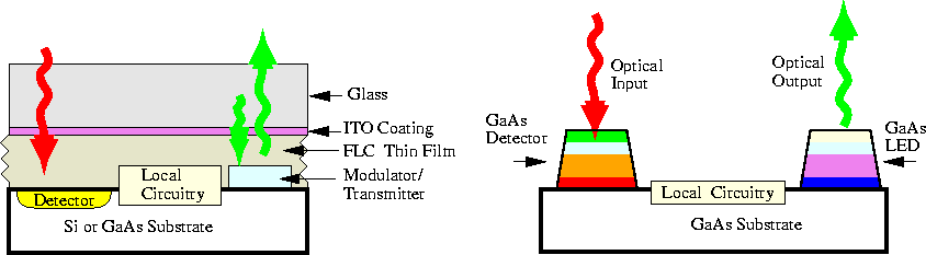
Figure 5.2: Smart light modulation using a) SLMs, b) GaAs receivers and LEDs
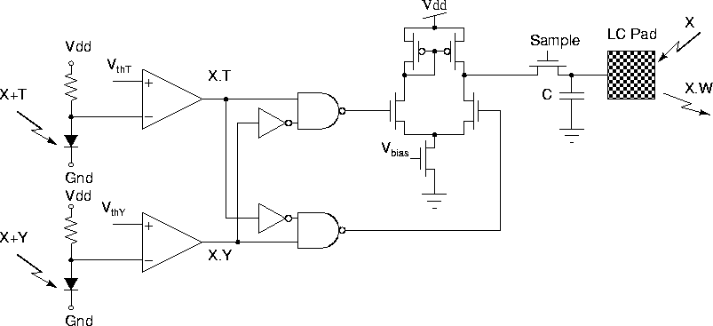
Figure 5.3: Pixel circuit of Yu et al.'s optical neuro-chip.