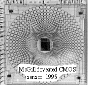
Wodnicki et al. have designed and fabricated a foveated CMOS sensor [Wodnicki et al. 95], which has a high resolution central region and a peripheral region with decreasing resolution. In the central region photodetectors are uniformly spaced in a rectangle and in the periphery are placed in a circular array (See Figure 2.16). Photodetectors have been realized using circular parasitic well diodes operating in integrating mode. The area of photodetectors in the circular outer region increases exponentially, resulting in the log-polar mapping, which is known to be both scale and rotation invariant.
The chip has been fabricated in a 1.2 ![]() m CMOS process. It has 16
circular layers in the periphery. The chip size is
4.8mm
m CMOS process. It has 16
circular layers in the periphery. The chip size is
4.8mm ![]() 4.8mm. It uses a 3.3 V supply voltage and dissipates
about 10 mW.
4.8mm. It uses a 3.3 V supply voltage and dissipates
about 10 mW.
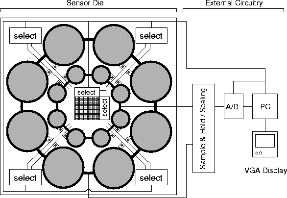
Figure: Simplified structure of Wodnicki et al.'s foveated CMOS
sensor and the test system.