Implementing a resistive network in VLSI can be achieved using passive
or active elements. In a CMOS process there are several passive
elements that can be used as resistor: diffusion resistance, well
resistance, and poly resistance![]() . All these elements have their own advantages and
disadvantages. However, the resistance values achievable using these
passive elements is far below what is needed in a resistive network. A
simple reason can be found from the power consumption point of view.
If the resistances are small, a large amount of power will be consumed
in the resistors, in order to have sufficiently large voltages at the
nodes of the network. Another reason is that the input currents are
usually very small, which then require large resistances to produce
large enough voltages detectable at the output. For example a typical
current of 10 nA requires a resistance of 100 MOhm to produce a 1 V
voltage difference.
. All these elements have their own advantages and
disadvantages. However, the resistance values achievable using these
passive elements is far below what is needed in a resistive network. A
simple reason can be found from the power consumption point of view.
If the resistances are small, a large amount of power will be consumed
in the resistors, in order to have sufficiently large voltages at the
nodes of the network. Another reason is that the input currents are
usually very small, which then require large resistances to produce
large enough voltages detectable at the output. For example a typical
current of 10 nA requires a resistance of 100 MOhm to produce a 1 V
voltage difference.
Therefore, it is clear that active resistors are needed for implementing resistive networks. There are many active resistor circuits, from which a large number operate in saturation region. Despite all efforts that has gone into designing resistors in the saturation region, they are not typically useful for resistive networks, as the dynamic range of these resistive circuits is small, and more importantly, cannot provide very large resistances (> 10 Mega Ohm).
Now we will have an overview on several resistive elements that have been used in some vision chips. The first circuit, which is known as HRES (Horizontal RESistor) [Mead 89b], is shown in Figure 7.34. It can be shown that in subthreshold region

where Io and n are process dependent parameters. In order to realize the voltage sources represented by Vbias, one of the circuits in Figure 7.35 can be used. Although ideally all these circuits seem to generate a voltage drop, controllable by the biasing currents Ibias, there are important notes to be given on each circuit.
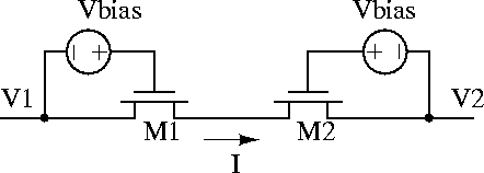
Figure 7.34: Schematic of the horizontal resistor.
The first circuit, which is used in the original HRES operates properly in almost all conditions when it is biased in subthreshold. However, if one of the inputs, say in1, is held at a low voltage, the output voltage of the associated OTA will stay at a constant voltage because the input branch is cut off. Therefore, the Vgs of M1 will exceed the desired value and a large current can pass through the resistor.
The second circuit (Figure 7.35-b) which is a simple source follower stage has a gain less than unity. This means that for large input voltages the voltage drop increases; hence, large currents may pass through the resistor. This circuit cannot be used for subthreshold operation, and in a few vision chips has been used in saturation region.
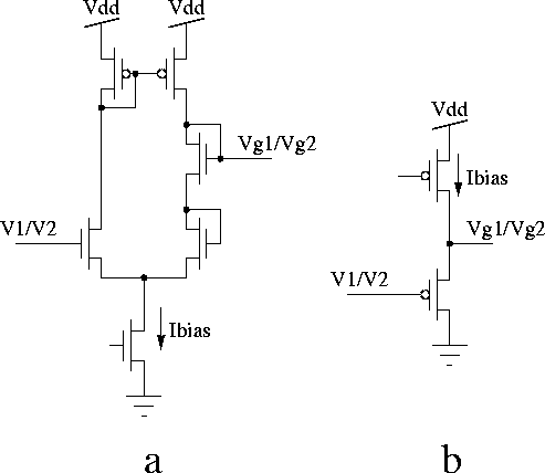
Figure 7.35: Two biasing circuits for the HRES.
Resistive fuses as described in section 2.15 are useful for image segmentation. Two circuits for implementing a resistive fuse were presented in the same section. Another circuit introduced by F.A. van Schaik [van Schaik 93] is a variation of the original HRES circuit, but with segmentation capabilities similar to resistive fuses, and without their local minimum problem. The main difference between this resistive circuit and HRES is that the input of the OTA is provided by a modulating voltage Vmodulation, as shown in Figure 7.36.
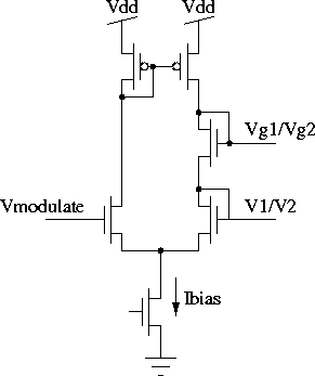
Figure 7.36: van Schaik's modulating resistor.