As device dimensions shrink, the quantum efficiency of the devices shift to shorter wavelengths. The effect can be seen in Figure 7.14, where the simulated quantum efficiency for three junction diodes and for six different processes are shown. The shift toward shorter wavelengths for scaled processes is because as the vertical dimensions get shorter, photogenerated electron-hole pairs contributing to photocurrents are those closer to the surface. Longer wavelength photons can contribute only if the junction is deep enough. These simulated quantum efficiency curves clearly indicate that the best junction diodes still covering a good proportion of the visible spectrum with sufficient quantum efficiency, are the diffusion-substrate and well-substrate junctions.
In reality scaled processes may use different material for diffusion and gate. For example silicided diffusion and gate is commonly used in almost all sub-micron processes to obtain low resistance. Silicide blocks most parts of the visual spectrum. In order to reduce the effect of silicides, they should either be masked out in the process, or make some windows through which light can get through to the semiconductor.
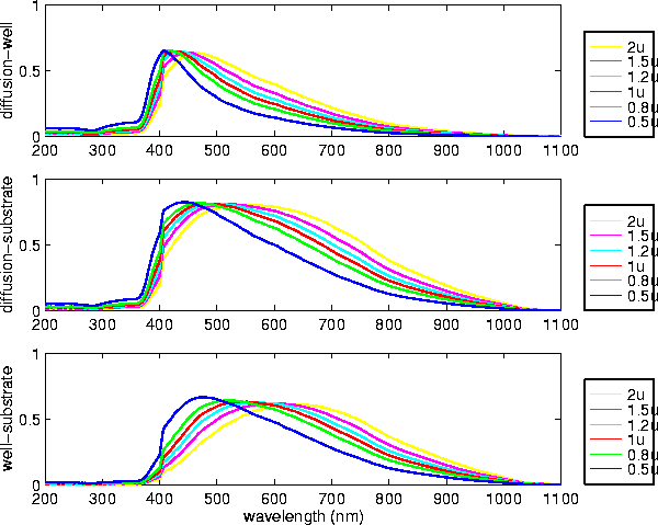
Figure 7.14: Quantum efficiency of three different vertical junction diodes for six
scaled processes.