The structure of a photogate is shown in Figure 7.12. A photogate is nothing but a MOS capacitor exposed to light. The principal operation of a photogate is integrating the photogenerated carriers in the depletion region, which is created by applying a large voltage to the gate. A simple assumption that we make here is that the depth of the depletion region is small. One can verify this using the following equation.
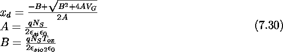
In a 2 ![]() m process the typical values for
m process the typical values for ![]() are less than
0.5
are less than
0.5 ![]() m.
m.
Therefore, it is reasonable to assume that all the charges filling the potential well are diffusing from areas outside the depletion region.
One important drawback of photogates is that they have very poor blue response because the gate material absorbs that part of the spectrum. In new processes (such as HP processes available through MOSIS) the gate is silicided, which even blocks most part of the visual spectrum. In these processes the silicide layer should be masked out from the areas above the photogate. Another solution is to make several windows in the gate so the light can pass through. Even with polysilicon gates it is recommended to use windowed gate for the photogate devices.
The spectral response of the photogate is simply obtained by solving the diffusion equation in the substrate area. Notice that a photogate works in a reset-and-integrate mode. At the reset cycle the potential well is emptied from charges. During the integration cycle diffusion of photogenerated currents fills up the potential well.
![]() is the photon flux at the surface of the silicon. If we
assume that the gate material is polysilicon and has the same
absorption coefficient as silicon, we will have:
is the photon flux at the surface of the silicon. If we
assume that the gate material is polysilicon and has the same
absorption coefficient as silicon, we will have:
![]()
The simulated spectral response of the photogate is shown in Figure 7.13. As is expected the device has a better response for the red part of the spectrum.
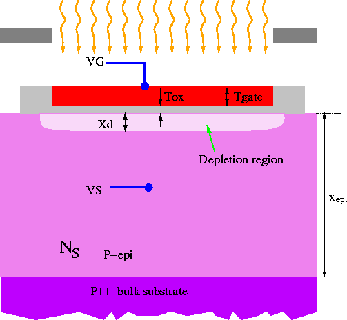
Figure 7.12: Structure of a photogate device in an N-Well CMOS process.
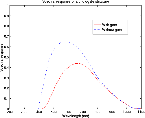
Figure 7.13:
Spectral response of the photogate.