Dynamic range in conventional charge integration-based imagers is limited by the integration time, which is global to all pixels in an imager. In [Hamamoto et al. 96a, Hamamoto et al. 96c, Hamamoto et al. 96b, Hamamoto et al. 97] Hamamoto et al. describe an imager which compresses the image using motion information (similar to the image compression sensor in section 3.23) and at the same time increases the dynamic range by controlling the integration time of individual pixels depending on the saturation status of the pixel.
The schematic diagram of the processing circuit is shown in Figure 3.34. Whenever the temporal change at the pixel exceeds a threshold, or the detector is saturated, a flag is turned on. Consequently, the pixel value is output and the detector is reset. If the flag is not activated the detector continues its charge integration operation until the flag is activated.
Current mode techniques have been used in the design of the processing
element. A column parallel architecture has been used for the chip
(See section 3.23). The fabricated chip has 32 ![]() 32
pixels in a 1P-2M 1
32
pixels in a 1P-2M 1 ![]() m CMOS process. The dimensions of the
detector, analog memory, and processing elements are
m CMOS process. The dimensions of the
detector, analog memory, and processing elements are ![]() ,
, ![]() , and
, and ![]() ,
respectively. The chip dissipates 150 mW of power and has a
processing speed of 2
,
respectively. The chip dissipates 150 mW of power and has a
processing speed of 2 ![]() .
.
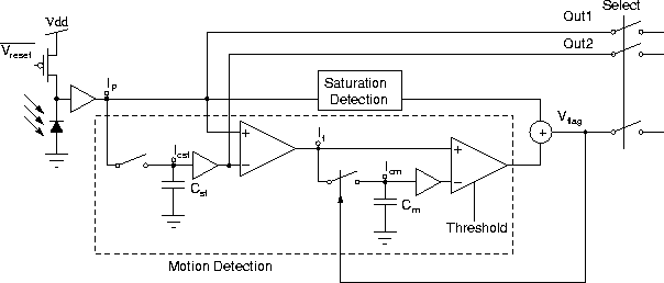
Figure: Processing circuitry in Hamamoto et al.'s motion adaptive
sensor.