This silicon retina is an implementation of the outer-plexiform of
retinal processing layers [Andreou and Boahen 94b, Boahen and Andreou 92]. The design has
a distinctive feature that separates it from all other silicon
retinas. The implementation uses a very compact circuit, which has
enabled the realization of a 210 ![]() 230 array of image sensors and
processing elements with about 590,000 transistors, which is the
largest among all reported vision chips.
230 array of image sensors and
processing elements with about 590,000 transistors, which is the
largest among all reported vision chips.
This silicon retina uses a diffusive smoothing network shown in Figure 2.8 [Andreou and Boahen 94b]. The function of this one-dimensional network can be written as
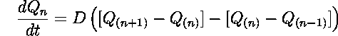
dQn/dt is the current supplied by the network to node n,
and D is the diffusion constant of the network, which depends on
the transistor parameters, and the voltage ![]() .
.
Andreou and Boahen have encapsulated the model of the retina in a neat and small circuit illustrated in Figure 2.9. This circuit includes two layers of the diffusive network. The upper layer corresponds to horizontal cells in retina and the lower layer to cones. Horizontal N-channel transistors model chemical synapses.
The function of the network can be approximated by the biharmonic equation
![]()
![]()
where g and h are proportional to the the diffusivity of the upper and lower smoothing layers, respectively. More details about the function of the circuit can be found in relevant references [Andreou and Boahen 94b, Boahen and Andreou 92].
Several versions of the 2D chip have been implemented using the
circuit shown in Figure 2.8. All the 2D chips use
a hexagonal network with six neighborhood connection. The largest chip
occupies an area of 9.5 ![]() 9.3, in a 1.2
9.3, in a 1.2 ![]() m CMOS process with
two layers of metal and poly. A cell size of about
m CMOS process with
two layers of metal and poly. A cell size of about ![]() has been achieved for this implementation. Under typical
conditions the chip dissipates 50mW.
has been achieved for this implementation. Under typical
conditions the chip dissipates 50mW.
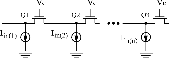
Figure 2.8: The diffusive network used in Andreou-Boahen's
silicon retina.
Figure 2.9: Schematic of the 1D silicon retina modeling the
outer-plexiform of retinal processing.