The simplest structure for storing charge is the DRAM style cell shown in Figure 7.37. However the leakage current of the source of the switch transistor limits the charge retention time, to up to a few seconds for digital DRAM storage cells. The acceptable retention time for an analog application obviously depends on the resolution required. Considering the resolution, the acceptable retention time drops from that for DRAM cells by two orders of magnitude (for 8 bit resolution by about 1/256). This circuit is useful only for very short term storage, such as in small imagers with fast frame rates.
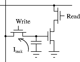
Figure 7.37: A DRAM style memory for storing analog charge. a) The
original
The storage capability of the cell can be improved by using several techniques, such as differential storage, and leakage reduction. In differential storage technique the original signal is translated into a differential signal and stored on two similar storage devices. As the leakage reduces the charge almost equally at both nodes, the difference remains the same. This method can increase the storage time by several times. A drawback of this technique is the additional area consumed by single ended-to-differential translation and the extra capacitance.
In leakage reduction techniques the leakage of the source/drain diffusion of the switching transistor at the storage node is reduced by setting the voltage across the anode and kathod of the source diffusion-well diode to zero [Vittoz et al. 91], as shown in Figure 7.38. Using this circuit storage times of up to several seconds in normal conditions can be achieved.
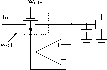
Figure 7.38: Circuit for reducing the leakage.
Floating gate structures have long been used in EPROM devices. Their storage capability for analog signals has also been used in many implementations of analog systems. Despite the long term storage achieved with floating gate structures (in the order of several years), the accuracy, programming, and reprogramming issues of these devices remain to be challenging. Floating gate devices can be found either in special processes, where thin-gate devices are available for low voltage programming, or in standard processes, where the gate of a normal transistor is left floating. The floating gate devices in standard processes require high programming voltages, which might exceed the breakdown voltages of different junctions in the process, or they may need accelerated mechanisms by exposing the chip to UV light. The accuracy achieved using floating gate devices is around 6 to 8 bits.