In continuous spatio-temporal processing chips, delay elements are
used to retain past information. Realizing ideal controllable delay
elements is very difficult, if not impossible. The delay element is
usually approximated by circuits, such as integrators.
Figures 7.39-a and 7.39-b show two
basic voltage mode circuits for delaying signals. Both circuits add
distortion both in phase and amplitude to the input signal. However,
this can be tolerated in many vision chips. The current mode delay
element in Figure 7.39-c has been used as an
essential building block in current mode circuits![]() .
.
The amount of delay in the RC network depends on the resistor value, in the OTA-C circuit on the bias current, and in the current-mode delay element on the input current level.
In order to achieve large delay times using a conventional OTA-C circuit, very small biasing currents are required. This imposes several problems, including increased mismatch at low current levels, and sensitivity to different noise sources. This requirement can be reduced by using linearization techniques applied to the OTA [Furth and Andreou 95, Moini et al. 97b].
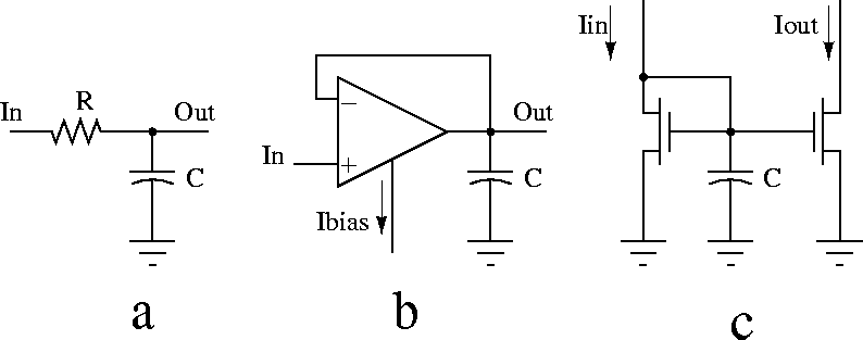
Figure 7.39: a) a RC circuit used as a delay element, b) an OTA-C circuit
as a delay element, c) a current mode delay element.