This silicon retina subtracts the original image from a spatially smoothed version of the image, therefore it eliminates the local average and enhances edges. This retina, however, uses ``well'' resistance in the resistive network used for smoothing operation [Wu and Chiu 95, Wu and Chiu 92]. Each cell consists of two parasitic phototransistors; one which is properly isolated from other transistors, and one whose base is shared with its neighboring phototransistors of the same type. The photogenerated electron-hole pairs in the latter can therefore diffuse to its neighbors, resulting in a smoothing function. The simplified layout of four cells of this retina is shown in Figure 2.24.
Due to the large stray capacitance and resistances associated with the base of sharing phototransistors, the smoothing operation will have a delay. Hence, a crude motion detection is also obtained.
The major drawback of such a retina is the uncontrollability of both the smoothing constants and the delay, which heavily depend on the process used, the size, and the shape of the well regions being shared by the sharing phototransistors.
A 32 ![]() 32 array of this silicon retina has been fabricated in a
0.8
32 array of this silicon retina has been fabricated in a
0.8 ![]() m DPDM CMOS process. Each cell occupies an area of 60
m DPDM CMOS process. Each cell occupies an area of 60 ![]() 60
60 ![]() .
.
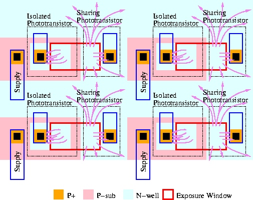
Figure 2.24: Simplified layout of Wu-Chiu's retina.