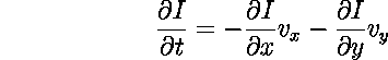
This 2D motion detection chip designed by Tanner and Mead [Tanner and Mead 88, Mead 89b] globally solves the optic flow equation
by feeding back the error
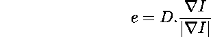
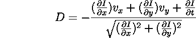
where
As is seen the algorithm used in the implementation of this chip is based on purely mathematical formulation of the optic flow derived by Horn and Schunck [Horn and Schunck 81] and modified by Hildreth [Hildreth 85].
The chip contains phototransistors, and temporal and spatial
differentiation circuitry for computing the spatio-temporal gradients
of the input image, ![]() ,
, ![]() ,
and
,
and ![]() .
.
The spatio-temporal information is collectively computed across the chip. The output of the chip is a global signal indicating the motion flow of the whole image (see Figure 3.3). Therefore, the chip is only capable of reporting a global motion. Figure 3.4 shows the block diagram of each motion processing element in Figure 3.3.
Despite some imperfections pointed out by others [Koch et al. 90], as one of the first vision chips being realized, this chip certainly demonstrated and proved that the low level vision processing based on mathematical algorithms can be implemented in VLSI.
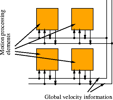
Figure 3.3: Architecture of Tanner and Mead's optic flow motion detector.
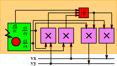
Figure 3.4: Block diagram of Tanner and Mead's motion detector elements.