Kramer et al.'s vision chip is a 1D motion detector [Kramer et al. 95].
The algorithm used in the implementation is rather intuitive, though
the basic element used is very similar to elementary motion detection
(EMD) units. The architecture of the motion detection unit is shown in
Figure 3.21. I represents the photodetectors
which use the Delbrück's adaptive
photocircuit [Mead 94], E, is the edge detection
circuit, P is a pulse shaping circuit, and M is the motion
computation element. The edge detection circuit E, which is shown in
Figure 3.22, issues an output current pulse on the
occurrence of an increase of the input light intensity. The output of
the edge detector is input to the pulse shaping circuit P, shown in
Figure 3.23, and two voltage pulses are generated.
One of them, ![]() , basically follows the shape of the input
current spike, while the other one,
, basically follows the shape of the input
current spike, while the other one, ![]() , only follows the
increasing edge and has a long decaying tail.
, only follows the
increasing edge and has a long decaying tail.
The motion detection unit M samples the ![]() output from one
channel by the
output from one
channel by the ![]() of the other channel. If there is no motion,
the
of the other channel. If there is no motion,
the ![]() outputs will be low. If there is a motion, for example
from detector 1 to detector 2, the output of unit
outputs will be low. If there is a motion, for example
from detector 1 to detector 2, the output of unit ![]() will detect a
none-zero value. The value of this voltage will be higher, if the time
between the start of the decay of
will detect a
none-zero value. The value of this voltage will be higher, if the time
between the start of the decay of ![]() and the
and the ![]() spike is shorter.
spike is shorter.
The chip has been designed and fabricated in a 2 ![]() m CMOS process.
Each cell takes an area of 50,000
m CMOS process.
Each cell takes an area of 50,000 ![]() . The chip has shown some
degree of robustness to contrast and light level variations.
. The chip has shown some
degree of robustness to contrast and light level variations.
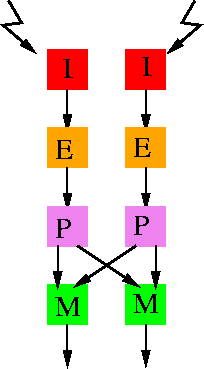
Figure: Architecture of Kramer et al.'s motion detection system.
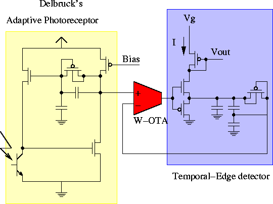
Figure: Kramer et al.'s temporal edge detection circuit.
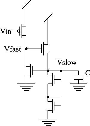
Figure 3.23: Circuit to generate a fast and a slowly decaying signal.