Achieving large dynamic range requires adaptation techniques for individual pixels. Global adaptation although improves the dynamic range, is still limited in many situations, where different parts of the image are very bright or very dark. The adaptive sensitivity CCD imager designed by the VLSI group in Technion improves the dynamic range by controlling the integration time of each individual sensor [Chen and Ginosar 95].
The pixel circuit with a set-reset flip-flop (SR-FF) is illustrated in Figure 6.1. The main difference between this photocircuit with conventional photogate-based photocircuit is the addition of the SR-FF.
The sensor is exposed to the light at several different integration times (for example with multiples of 1, 8, and 64). First all the SR-FFs in the pixels are set using the ``global set'' signal. Then the shortest integration is performed. If a pixel is detected saturated during any integration cycle, or is likely to saturate in the next cycle, its associated flip-flop is reset for the following cycles. Resetting pixels which can get saturated has the additional benefit of avoiding blooming. After the integration cycles are finished the images is read out using interline CCD transfer.
The fabricated prototype chip has 9 ![]() 16 pixels in a 2
16 pixels in a 2 ![]() m
CMOS/CCD process, in a TINY chip (2.22mm
m
CMOS/CCD process, in a TINY chip (2.22mm ![]() 2.22mm).
2.22mm).
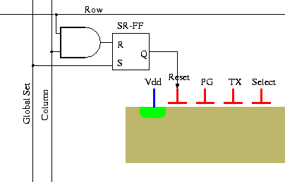
Figure 6.1: Pixel schematic of the adaptive sensitivity imager.