The correlation based motion detector of Delbrück [Delbrück 93c] unlike some other motion detection systems, which depend on spatial and temporal differentiation, uses correlation to extract motion information, and hence claims to be more robust than other motion detectors. The structure of the chip is depicted in Figure 3.8. The signal from a detector is delayed by the delay element and is compared with a reference level. As indicated in the figure there is only one sensitive direction. Motion in the other direction may be detected by another delay-and-compare element in the other direction. The chip has an array of photodetectors, time delay elements, and antibump circuits.
The outputs from delay elements are collectively mixed with the outputs of the photodetectors through capacitive coupling. When a part of image moves at a velocity that matches the delay time of the delay elements and the spatial separation between adjacent photodetectors, the signals at each stage get constructively added together and grow in size as they pass through the array.
A difference between this approach and the elementary motion detection (EMD) methods is that in EMD methods only two contiguous cells take part in the motion detection process, but in Delbrück's approach all the previous cells affect the output of the motion detection.
Delbrück has implemented a hexagonal 2D [Delbrück 93c] motion sensor. Photodetection is performed by a novel adaptive photodetector circuit shown in Figure 3.9. The output of the motion detector is obtained from an antibump circuit, which provides a nonlinearity function [Mead 94, Delbrück 93c, Delbrück 93b].
The 2D chip contains 26 ![]() 26 cells in an area of
6.9mm
26 cells in an area of
6.9mm ![]() 6.8 mm, using a 2
6.8 mm, using a 2 ![]() m CMOS process.
m CMOS process.
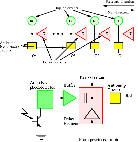
Figure 3.8: Top: the architecture, bottom: the schematic diagram of a cell of
Delbrücks's motion detector.
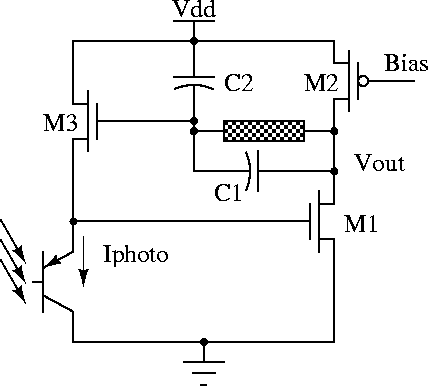
Figure 3.9: The circuit diagram of the adaptive photodetector. The shaded
box contains the adaptive element.